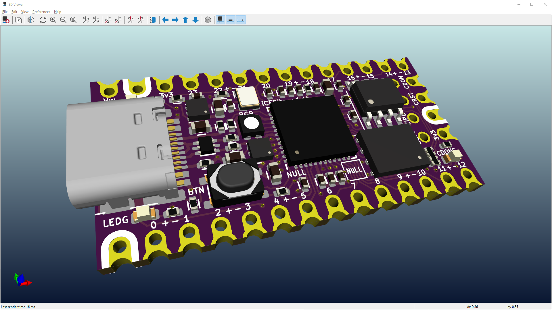
https://media.licdn.com/dms/image/C5112AQHZ8u0OAuILFA/article-inline_image-shrink_1000_1488/0/1531881377738?e=1683158400&v=beta&t=rW0GjEonBbfGtktoZMS3J8WzP_L33iT_o68rhNsbv4o
Table of Contents:
Crash Course Preface:
This notion page is meant to serve as an introductory guide into the creation and manufacturing of PCB’s or Printed Circuit Boards. This guide will show you good practices and guidelines to follow when creating a PCB following the completion of a schematic.
Sections 1 - 10 Provide a brief introduction into what an actual PCBA is and some context to consider before beginning the whole process
1. Introduction
When creating a PCBA, it is important to follow good practices to ensure that the final product is reliable, functional, and safe. The PCBA manufacturing process typically involves designing the PCB layout, selecting components, assembling the board, and testing and validating the final product.

This step always should follow the creation of a schematic. This is to ensure that you can import all the parts needed to meet product specifications
2. Design Considerations
Designing a PCB layout that is optimized for manufacturability and reliability is crucial for the success of the project. Here are some design considerations to keep in mind:
PCB layout guidelines
- Use standard PCB footprints to ensure compatibility with PCB assembly equipment
- Minimize the number of vias and keep them away from sensitive components to avoid signal interference
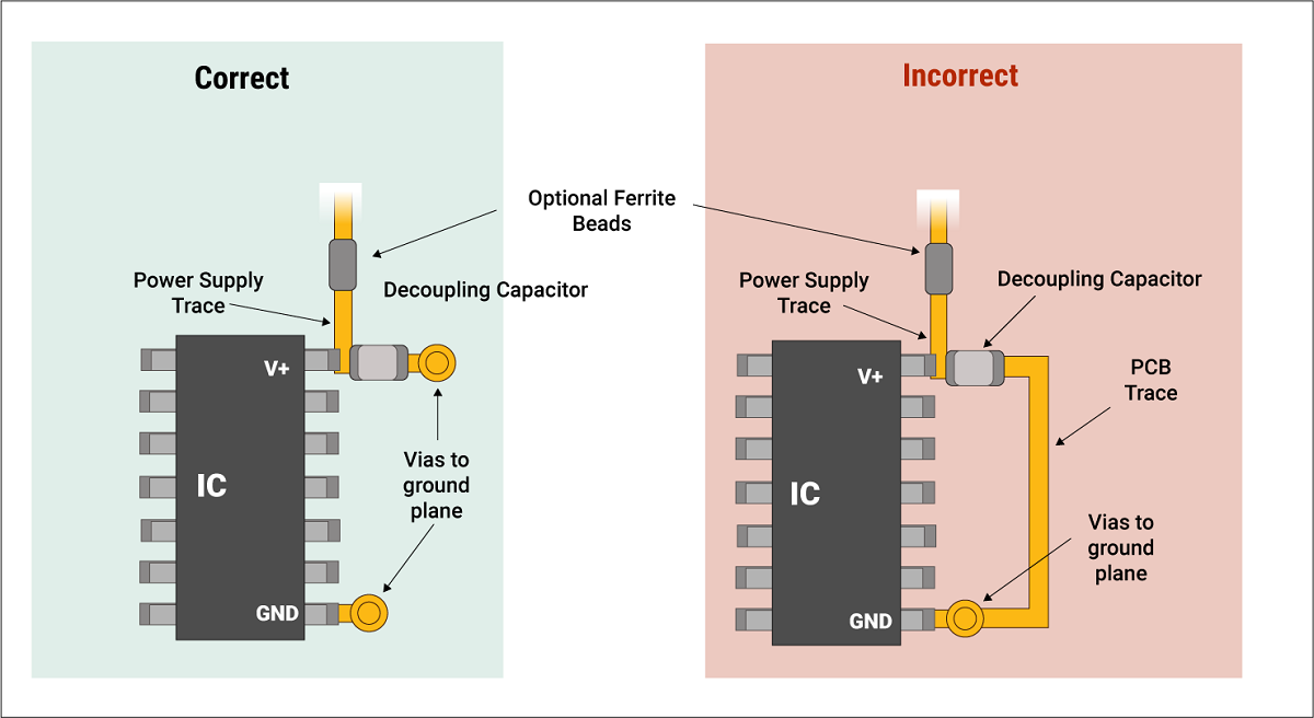
- Place decoupling capacitors close to the power pins of each component to reduce noise and voltage fluctuations

Proper decoupling capacitor placement. It is important to also reference a ground plane via something called a via which is a hole to another plane or ground pour in another layer of the board
Component selection
- Choose components that are rated for the desired operating conditions (temperature, voltage, etc.)
- Consider the availability and cost of components when selecting them
- Use components from reputable manufacturers to ensure quality and reliability
Thermal management
- Proper thermal management is essential for components that generate heat, such as power amplifiers, voltage regulators, and microprocessors.
- Consider the use of thermal vias, heat sinks, and thermal pads to dissipate heat and maintain component temperatures within safe operating limits.
EMI/RFI considerations
- Minimize the length of traces carrying high-frequency signals to reduce electromagnetic interference (EMI) and radio-frequency interference (RFI)
- Use shielding techniques such as grounded metal cans or shielding tape to reduce EMI/RFI
3. Assembly process
The assembly process involves soldering the components to the PCB and ensuring that the board is functional and meets the required quality standards.
*It should be noted that for simpler boards, the assembly can be done by the engineer soldering all the parts on. In industry, PCB’s get much more complicated so the assembly of the components on the board will be done via a fabrication house.
Soldering techniques
- Use a high-quality solder paste with the correct particle size for the components being soldered
- Use a consistent and repeatable soldering process to ensure consistent quality
- Consider the use of solder paste stencils to apply a precise amount of solder paste to each component
Quality control
- Perform visual inspections to ensure that components are properly aligned and soldered
- Use automated optical inspection (AOI) or X-ray inspection to detect defects that may be missed during visual inspections
- Implement a robust quality control system to ensure that all boards meet the required quality standards
Testing and Validation
- Test the functionality of the board using appropriate test equipment and procedures
- Perform environmental testing (temperature, humidity, vibration, etc.) to ensure that the board is reliable in a range of conditions
- Validate that the board meets the required performance specifications
